
| Key product |
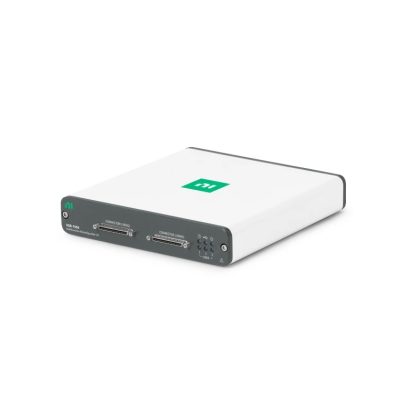
| Analog Input (AI) Channels: 8 Input Modes: Differential (DIFF), Non-Referenced Single-Ended (NRSE), Referenced Single-Ended (RSE) (software-selectable) ADC Type: Successive Approximation Register (SAR) Resolution: 16 bits Conversion Time: 2 µs per channel Maximum Sampling Rate: 500 kS/s per channel Input Impedance: Powered On: 1.25 GΩ || 2 pF Powered Off/Overload: Minimum 4.0 kΩ Input Signal Range: ±1 V, ±2 V, ±5 V, ±10 V (software-selectable) Input Bias Current: ±5 nA Input Offset Current: ±5 nA Input Coupling: DC Overvoltage Protection: Powered On: ±42 V maximum Powered Off: ±35 V maximum Absolute Accuracy (Calibrated) at Full Scale: ±10 V: 2,283 µV ±5 V: 1,170 µV ±2 V: 479 µV ±1 V: 252 µV Absolute Accuracy (Uncalibrated) at Full Scale: ±10 V: 36,895 µV ±5 V: 19,018 µV ±2 V: 7,667 µV ±1 V: 3,769 µV Dynamic Characteristics: Bandwidth: Small Signal: 1 MHz, Large Signal: 500 kHz Crosstalk: -80 dB, DC to 100 kHz Settling Time: Ranges from 0.5 µs to 12 µs depending on the range and step size Analog Output (AO) Channels: 8 Output Type: Single-ended, voltage output Resolution: 16 bits Update Time: 1.0 µs Maximum Update Rate: 1 MS/s DAC Type: Enhanced R-2R Range: ±10 V Output Coupling: DC Output Impedance: 0.5 Ω Current Drive: ±2.5 mA Overvoltage Protection: Powered On: ±15 V maximum Powered Off: ±10 V maximum Absolute Accuracy (Calibrated) at Full Scale: ±10 V: 2,498 µV Absolute Accuracy (Uncalibrated) at Full Scale: ±10 V: 40,941 µV Dynamic Characteristics: Settling Time: Ranges from 1.8 µs to 7.8 µs depending on step size and accuracy Slew Rate: 10 V/µs Noise: 250 µVrms, DC to 1 MHz Digital I/O Channels: Connector 0: 32 channels, 80 MHz maximum frequency Connector 1: 16 channels, 10 MHz maximum frequency Logic Family: LVTTL, LVCMOS (user-selectable) Default Software Setting: 3.3 V Digital Input Logic Levels: Input Low Voltage (VIL, Maximum): 0.42 V to 0.80 V depending on logic family Input High Voltage (VIH, Minimum): 0.84 V to 3.00 V depending on logic family Digital Output Logic Levels: Output Low Voltage (VOL, Maximum): 0.20 V to 0.40 V depending on logic family Output High Voltage (VOH, Minimum): 1.00 V to 3.00 V depending on logic family Input Leakage Current: ±15 µA maximum Output Current: Source and Sink: 4 mA Digital I/O Voltage Switching Time: 2 ms maximum FPGA Type: Kintex-7 160T Number of Flip-Flops: 202,800 Number of LUTs: 101,400 Embedded Block RAM: 11,700 kbits Number of DSP48 Slices: 600 Timebase: 40 MHz, 80 MHz, 120 MHz, 160 MHz, or 200 MHz Timebase Accuracy: ±100 ppm Bus Interface USB Compatibility: USB 2.0 Hi-Speed or Full-Speed Data Transfers: DMA, interrupts, programmed I/O Number of DMA Channels: 3 Power Requirement Input Voltage: 9 V to 30 V Maximum Power: 20 W Overvoltage Protection: 40 V Physical Characteristics Dimensions: 18.5 cm × 17.3 cm × 3.6 cm Weight: 1,000 g I/O Connectors: 2 × 68-pin VHDCI Safety and Compliance Safety Voltages: Channel-to-Earth: ±12 V, Measurement Category I Channel-to-Channel: ±24 V, Measurement Category I Compliance: Meets IEC 61010-1, EN 61010-1, UL 61010-1, CSA C22.2 No. 61010-1 |


Reviews
There are no reviews yet.